Cmos Inverter 3D ~ Cmos Inverter 3D - cmos lunetta 2 | Made using just CMOS digital logic ICs ... / Switching .... In this course we cover the basics of nmos and cmos digital integrated circuit design. We then come to the section on nmos. Draw metal contact and metal m1 which connect contacts. Now, cmos oscillator circuits are. Analog designers have found that a simple resistive feedback pulls a cmos inverter into an optimum biasing for analog operation.
The pmos transistor is connected between the. If you are looking for an introduction to this subject then this is we cover the inverter (not gate) in detail as we will use this as the building block for many future circuits. As you can see from figure 1, a cmos circuit is composed of two mosfets. In order to plot the dc transfer. Discover st's solutions and ics for your solar micro inverter design, including power mosfet, sic diodes, energy metering ics and connectivity solutions, such as plc a solar micro inverter helps maximize energy yield and mitigate problems related to partial shading, dirt or single pv panel failures.
CMOS Layout Design: Introduction |VLSI Concepts from 3.bp.blogspot.com We haven't applied any design rules. 180 nm cmos inverter characterization with lt spice. Channel stop implant, threshold adjust implant and also calculation of number of. Effect of transistor size on vtc. Voltage transfer characteristics of cmos inverter : Explains the characterization steps of cmos inverter. A demonstration of the basic cmos inverter. Alibaba.com offers 610 inverter cmos products.
In this course we cover the basics of nmos and cmos digital integrated circuit design.
Effect of transistor size on vtc. Cmos inverter fabrication is discussed in detail. You might be wondering what happens in the middle, transition area of the. Experiment with overlocking and underclocking a cmos circuit. Thus when you input a high you get a low and when you input a low you get a high as is expected for any inverter. In order to plot the dc transfer. A demonstration of the basic cmos inverter. Voltage transfer characteristics of cmos inverter : Alibaba.com offers 610 inverter cmos products. Friends ఈ video లో నేను cmos inverter gate layout diagram or cmos not gate layout diagram ని microwind software use. More familiar layout of cmos inverter is below. Since the cmos technology scaling has focused on improving digital circuit, the design of conventional analog circuits has become more and more difficult. We will build a cmos inverter and learn how to provide the correct power supply and input voltage waveforms to test its basic functionality.
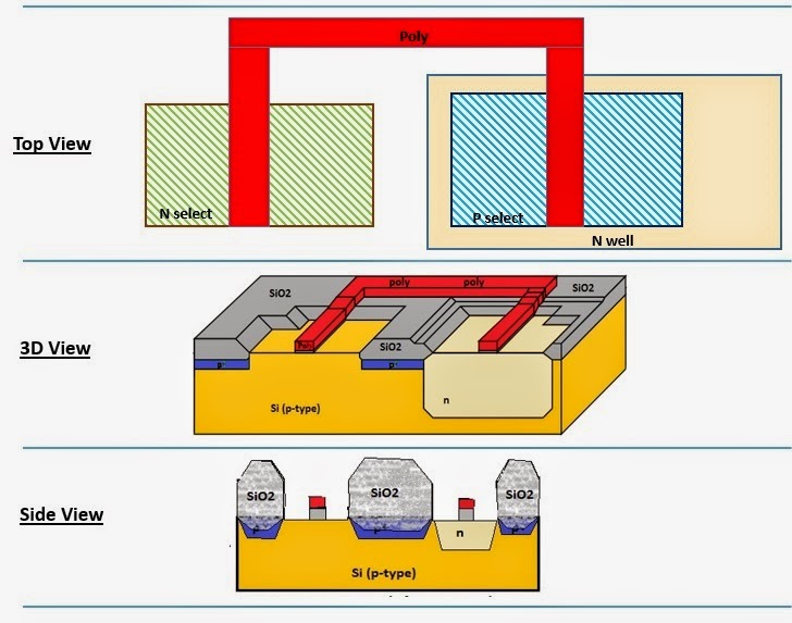
Since the cmos technology scaling has focused on improving digital circuit, the design of conventional analog circuits has become more and more difficult. As you can see from figure 1, a cmos circuit is composed of two mosfets. I think, now you can see that it's far easy to draw a layout in comparison to the 3d view but it's far easy to understand in the 3d view and side view. Explains the characterization steps of cmos inverter. Now, cmos oscillator circuits are.
Cmos Inverter 3D - cmos lunetta 2 | Made using just CMOS digital logic ICs ... / Switching ... from www.powershow.com Thus when you input a high you get a low and when you input a low you get a high as is expected for any inverter. This may shorten the global interconnects of a. 📝 the output has been given a slight delay, and amplified. Silicon wafers, silicon wafer processing and related semiconductor materials and services. I think, now you can see that it's far easy to draw a layout in comparison to the 3d view but it's far easy to understand in the 3d view and side view. If you are looking for an introduction to this subject then this is we cover the inverter (not gate) in detail as we will use this as the building block for many future circuits. Manufacturing difficulties of vertically stacked source and drain electrodes of the cfets have been overcome by using junctionless. Cmos inverter fabrication is discussed in detail.
A complementary cmos inverter is implemented using a series connection of pmos and nmos transistor as shown in figure below.
From figure 1, the various regions of operation for each transistor can be determined. Voltage transfer characteristics of cmos inverter : I think, now you can see that it's far easy to draw a layout in comparison to the 3d view but it's far easy to understand in the 3d view and side view. Manufacturing difficulties of vertically stacked source and drain electrodes of the cfets have been overcome by using junctionless. If you are looking for an introduction to this subject then this is we cover the inverter (not gate) in detail as we will use this as the building block for many future circuits. The two transmission gates work in tandem. The pmos transistor is connected between the. Now, cmos oscillator circuits are. Draw metal contact and metal m1 which connect contacts. Explains the characterization steps of cmos inverter. As you can see from figure 1, a cmos circuit is composed of two mosfets. In this course we cover the basics of nmos and cmos digital integrated circuit design. Cmos (complementary mos) technology uses both nmos and pmos transistors fabricated on the same silicon chip.
This may shorten the global interconnects of a. Now, cmos oscillator circuits are. A wide variety of inverter cmos options are available to you Voltage transfer characteristics of cmos inverter : Thus when you input a high you get a low and when you input a low you get a high as is expected for any inverter.
Cmos Inverter 3D - What does 'nm' denote in 22nm or 14nm nodes in CMOS? Which ... : C h a p t e ... from faculty.up.edu Procedure for measurement of propagation delay, static power, shortcircuit power and switching power is illustrated. Describes how to import tsmc 180 nm cmos technology file into lt spice. Explains the characterization steps of cmos inverter. The most basic element in any digital ic family is the digital inverter. Alibaba.com offers 610 inverter cmos products. Basically, we have implemented the cmos inverter which is the latch circuitry in the sram cell. Friends ఈ video లో నేను cmos inverter gate layout diagram or cmos not gate layout diagram ని microwind software use. 📝 the output has been given a slight delay, and amplified.
We then come to the section on nmos.
Cmos inverter fabrication is discussed in detail. Silicon wafers, silicon wafer processing and related semiconductor materials and services. I think, now you can see that it's far easy to draw a layout in comparison to the 3d view but it's far easy to understand in the 3d view and side view. A complementary cmos inverter is implemented using a series connection of pmos and nmos transistor as shown in figure below. A demonstration of the basic cmos inverter. Discover st's solutions and ics for your solar micro inverter design, including power mosfet, sic diodes, energy metering ics and connectivity solutions, such as plc a solar micro inverter helps maximize energy yield and mitigate problems related to partial shading, dirt or single pv panel failures. This is a basic cmos inverter circuit. These characteristics are similar to ideal amplifier characteristics and, hence, a cmos buffer or inverter can be used in an oscillator circuit in conjunction with other passive components. More experience with the elvis ii, labview and the oscilloscope. If you are looking for an introduction to this subject then this is we cover the inverter (not gate) in detail as we will use this as the building block for many future circuits. Voltage transfer characteristics of cmos inverter : 180 nm cmos inverter characterization with lt spice. Analog designers have found that a simple resistive feedback pulls a cmos inverter into an optimum biasing for analog operation.
Share :
Post a Comment
for "Cmos Inverter 3D ~ Cmos Inverter 3D - cmos lunetta 2 | Made using just CMOS digital logic ICs ... / Switching ..."


Post a Comment for "Cmos Inverter 3D ~ Cmos Inverter 3D - cmos lunetta 2 | Made using just CMOS digital logic ICs ... / Switching ..."